
Check out the project on GitHub.
During the last few months, two interesting opportunities coincided: First, I was asked to design a purpose-built electrical control board for a water pumping system. In addition, I had an idle offer for financial sponsorship waiting in my inbox. This finally gave me a reason and the means to expand my PCB design skills and venture into PCB assembly.
Electrical Safety Disclaimer: I try to do my best in terms of design for electronic safety and compliance, but PCB design continues to be just a hobby of mine. Although I have a few years of experience, my formal education is in computer science, not electrical engineering. Because of these reasons you should take all my designs with a grain of salt, and verify them by yourself if you plan to use them in any way. Especially since this project can be used with mains voltage, I take no responsibility for damages or injuries – you have been warned.
Transparency Disclaimer: This project has been financially supported by the PCB manufacturing company PCBWay. In exchange, I agreed to publish a written review of their services on my blog (see below) and link to their website. I required that I would be free to publish my personal unbiased opinion, without them influencing the review. They agreed, and a sponsorship was confirmed. They did however ask me to redact the name of the component distributor due to competition concerns.
Motivation and Requirements
As mentioned in the introduction, I was kindly asked to design a new water pump controller for a local urban gardening community project. Because my membership and work these is inherently voluntary, I was especially happy about the sponsorship. Although the design is released open-source and licensed under the terms of the MIT license, I can image selling these boards to make a few bucks of my development time and work (however, EU CE certifications are non-trivial to say the least). Due to this idea in the back of my mind, I designed a more general board than what would have been strictly necessary.
In any case, the water pump situation requires a least three switchable high-current DC channels and a method of monitoring the current flowing. This is to alert the operator when a pump fails or runs dry. The existing solution of several “Arduino-compatible” modules somehow wired together was not enough and reliable anymore, and a dedicated integrated solution was required. Additionally, a controller upgrade to a network-capable device is planned, so the board has to work with various host controllers.
I added a fourth backup channel in case a relay fails and also additional digital and analog IO connectors for potential auxiliary modules (such as flow meters or cooling fans) in the future. The whole system is interfaced via the Inter-Integrated circuit (I2C) protocol, enabling the usage with a wide variety of hosts like e.g. Arduinos and Raspberry Pis.
Circuit Design
The main goal is to safely switch high DC loads, without destroying the controller or endangering the environment or operator.
To switch and isolate the high-current channels, magnetic relays are used. These are in turn galvanically isolated from the main logic via optocouplers and also employ a fly back diode to protect against transient switching power spikes. Small red LEDs indicate the relay status.
The common pin of relay is connected to a current measuring IC each. These ICs measure the current flowing though them by measuring the magnetic field strength produced by an integrated low-resistance coil using a hall-effect sensor. In comparison to a shunt-resistor type measurement circuit this approach has the benefit of physical separation of the high current side and a low power draw, but comes at the cost of magnetic interference sensitivity and a natural resonance frequency, which has to be filtered, reducing the bandwidth.
Thanks to this multi-stage isolation the high currents are completely physically separate from the control logic. To prevent arcing, the recommended trace spacing of about 3 mm is used. To prevent power creepage due to corrosion or moisture across the board, slots are cut into the PCB. To prevent excessive heat generation which could lead to failure of the copper traces, double the normal amount of copper (2oz) is used. This is also a requirement for the targeted high-power trace width.
To control the relays, a I2C-capable general purpose input-output (GPIO) controller is used. To report the sensor values back to the host, a I2C-capable analog-to-digital converter (ADC) is used.
Relay Driver
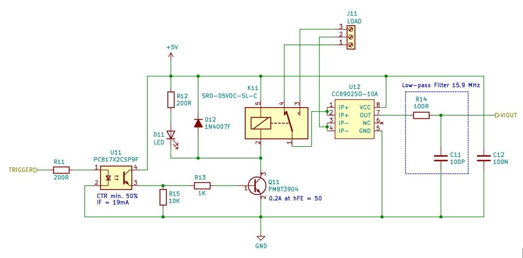
As explained before, the relay (K11) uses a optocoupler (U11) to isolate the sensitive micro controller IO port (TRIGGER) from any power pikes. However, the maximum output current draw of such an optocoupler is typically way smaller than what the coil of a relay requires to actuate. Because of this, a second stage is used in form of a NPN doted bipolar junction transistor (BJT) (Q11), kind of like a Darlington transistor. The transistor switches the supplied 5 Volts (+5V) to the relay coil when a signal from the optocoupler is received at the base of the transistor. An additional resistor (R15) is used as a pull-down to ground (GND) for the base, in case the microcontroller or optocoupler output is floating.
The optocoupler driving circuit delivers about 19 mA to the LED of the optocoupler using a series resistor (R11), which equates to about 10 mA output current for the specified worst-case current-transfer ratio (CTR) of 50%. Thus, the transistor has to be able to switch the required 70 mA for the relay coil when 10 mA are applied to its base. The transistor chosen has a minimum current gain (hFE) of about 50 in this application, which would enable it to switch up to 500 mA. To protect the transistor base, a resistor limits the base current to about 4 mA, which still enables a load switching of 200 mA – the rated current limit of the transistor.
When a relay switches off, the internal magnetic coil dumps its stored energy back into the circuit, acting as an inductor. This can and does lead to high power spikes, which can destroy the driving transistor and even arc across traces. This fly-back current is caught and dissipated by a fly-back diode (D12) placed in reverse polarity across the relay in parallel. During normal operation, it blocks and essentially acts as a cut wire, but once the coil unloads its energy it provides a path for the high current, “shorting” the coil. Depending on the resistance of the diode and the coil, the spike energy is the converted into heat and dissipated by the diode and coil. Due to this and depending on the target switching frequency, a large enough diode must be chosen.
The red indicator LED (D11) is placed in parallel across the relay as well, with a series limiting resistor (R12). During a fly-back current spike, the LED acts blocking due to its forward orientation.
Current Measurement
A hall-effect current measuring IC (U12) has its coil connected across the COM pin of the relay, enabling current measurements no matter what state of the relay is regarded as active. Due to the inductance of the internal coil, a small RC-filter for the output signal (VIOUT) is recommended by the manufacturer. This low-pass filter uses one resistor (R14) and one capacitor (C11) and is designed for a cutoff frequency of about 15.9 MHz. An additional decoupling capacitor (C12) is placed across the power supply of the sensor IC to smooth out small power irregularities.
Due to the inherent nature of magnetic relays, the inductive current measuring ICs and also the ADCs experience a measurement offset while the relays are energized. It is recommended to measure the actual load at a distance from the board, in order to obtain reference values. These reference values should then be used to compute an offset or function for each channel and amount of relays energized. For a table of experimentally found offset values, see the GitHub project page.
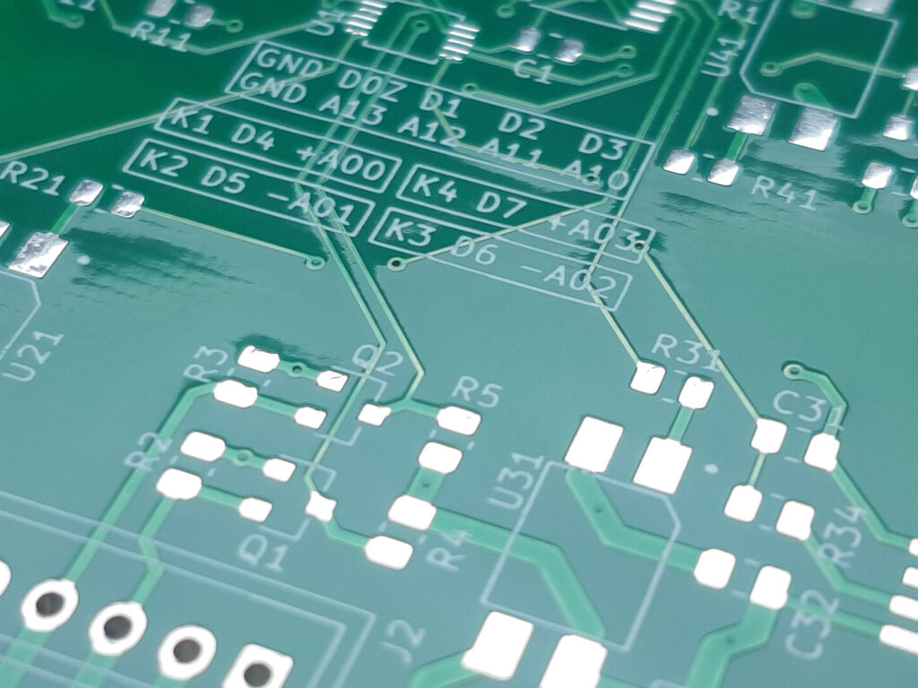
Digital Output and Input
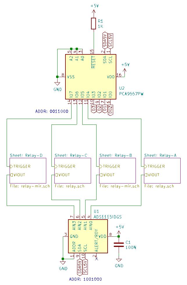
To trigger the optocouplers, a eight-channel GPIO chip with an I2C interface (U2) is used. The high four channels 4-7 are connected to the optocouplers, switching the relays. The low four channels 0-3 are connected to a JST-XH breakout header (DIGITAL). The chip is held in operating mode using a pull up resistor (R1) at its reset pin, and its I2C address is configured to be 0011000 by connecting all the address selection pins to ground (GND).
In order to provide the measured currents to the host, a 16-bit 4-channel ADC with an I2C interface (U1) is used. Its I2C address is configured to be 1001000 by connecting its address configuration pin to ground. A decoupling capacitor (C1) across its power supply is used to smooth the power supply and its effect on measurements. This ADC is capable of differential input, however the relay current measurements are single-ended by default.
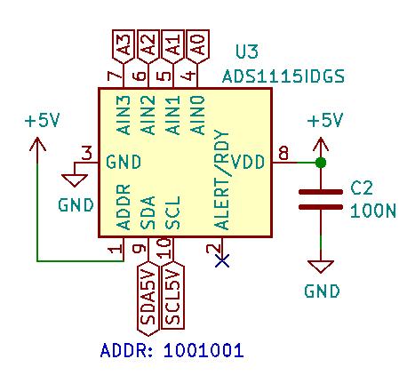
A second, identical ADC (U3) with a configured address of 1001001 (The address selection pin is connected to +5V) is connected to a JST-XH breakout header (ANALOG), providing four ADC input for flexible use. It too uses a decoupling capacitor (C2).
The I2C Bus
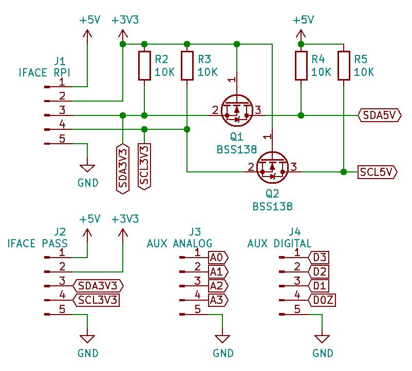
As mentioned before, the GPIO IC and the two ADCs are connected to a single shared I2C bus, being selected by using their respective I2C addresses. To enable the usage of the I2C with signal levels of both 3.3 Volt or 5 Volt, an I2C level-shifter is integrated into the circuit. The design of this level-shifter is mainly based on the AN10441 application notice by NXP, which has been proven to work in products such as the Adafruit I2C level-shifter.
Essentially, two logic-level metal-oxide-semiconductor field-effect transistors (MOSFETs) (Q1 and Q2) use pull up resistors to raise the voltage level of the I2C logic lines to either 3.3 Volts (+3V3, using R2 and R3) (SDA3V3 and SCL3V3) or 5 Volts (+5V, using R4 and R5) (SDA5V and SCL5V). For further details, see section “2.1.1 Operation of the level shifter” in the aforementioned application note.
All I2C devices on the board operate with a logic I2C level of 5 Volts. This was a conscious design decision, as these devices base their I2C logic voltage levels on the supply power voltage. Although the devices would function at a 3.3 Volt supply (and would then accept 3.3 Volt I2C signals), The 3.3 volt supply of host devices such as Arduinos or Raspberry Pis is typically rated only for a very low current. However, a suitably high current is required to switch the relays, thus the 5 Volt (+5V) supply (which can typically source a lot more current, about 300 - 500 mA) is required. Now, if the 5 Volt supply is required anyway, I2C might just as well based on it – this enables the user to leave the 3.3 Volt power supply (+3V3) disconnected if the host I2C logic levels are already 5 Volts, skipping the level-shifter and removing the requirement of two separate power rails in board design.
The I2C bus is connected to a JST-XH breakout header (IFACE RPI), and also passed though to a second header (IFACE PASS).
PCB Design
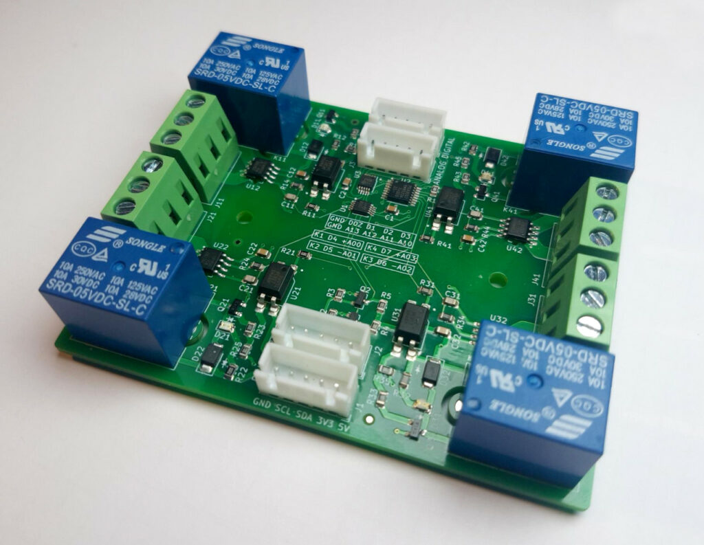
Before the actual printed circuit board (PCB) could be designed, all the components had to be chosen. Because I used a turn-key manufacturing contract, where the PCB fabricator sources all the components and parts, some thought had to go into distributor choice and availability. All parts were chosen in their surface-mount variant, to keep part and assembly cost down. The only through-hole components are the connectors and the relays.
I chose a large component distributor, which had all the parts I needed (or at least equivalents I could design for) in stock at a reasonable price, even during the ongoing silicon shortage of 2021. More importantly, they are based in Asia, to be precise in Shenzhen, China – the same city my chosen PCB manufacturing service PCBWay is based in. This dramatically reduces component shipping time. Sending the components on a round-trip across the globe from my country Germany to China would not only be slow but also expensive and wasteful – especially considering the components are made in China in the first place.
I had to accept a few minor compromises, for example I had to use a Chinese version of the originally planned current measurement chip (which was not in stock). The chip itself is great, but its datasheet is only available in Chinese. Even though I (tried to) learn Mandarin for a year, I had to resort to Google translate – no problem that cant be solved with modern technology. Some other components also had Chinese datasheets, but those were easy enough to read without machine translations as they were mainly mechanical drawings. I also used third-party JST-XH headers with a pin spacing of 2.54 mm instead of the planned genuine JST header with a pin spacing of 2.50 mm. This was due to availability at the manufacturing plant and lower cost.
I did not specify the exact model and manufacturer of simple passive parts like resistors and capacitors, instead giving the SMD assembly line engineers at PCBWay the option to use parts from their stock which conformed to my specifications.
I estimated the total bill of materials for a single board to come out a bit lower than $25, which is reasonable considering the expensive ADCs. In the future, these could be replaced with a cheaper, although probably less feature-rich alternative. It is important to note that many, if not all parts have a certain minimum order quantity – sometimes an entire reel, which increases upfront cost.
For the detailed bill of materials (BOM) and also the electrical ratings of the components, see the GitHub project page. There you can also find the BOM selection by the manufacturer in the fabrication files.
Board Layout
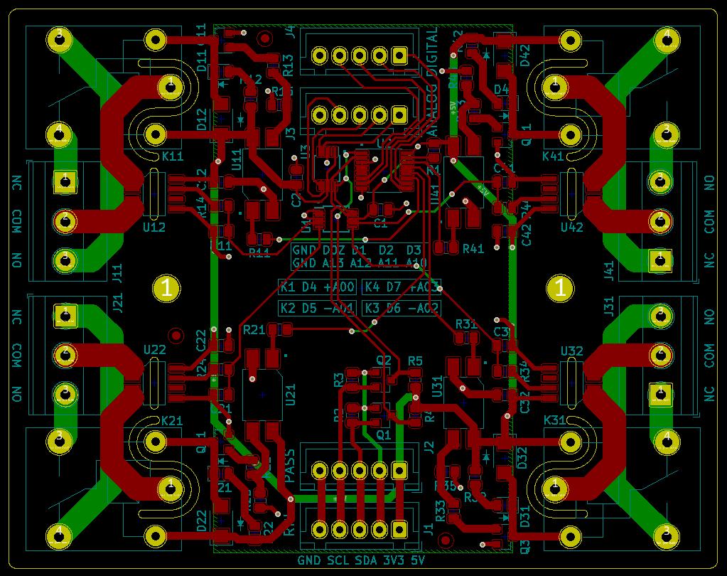
The PCB is a simple dual-side board with double-weight (2oz) copper plating with vias and plated holes. I chose lead-free finishing and soldering, as I’ll eventually have to conform to the EU RoHS directive should I ever sell these boards. Surface-mount parts are placed only on the top layer, and though-hole components are soldered only to the bottom layer. This simplifies the manufacturing process.
A ground plane is used below the low-voltage / logic circuity, but not below the high voltage sections to prevent arcing and shorts. The top side has no ground plane, because the top layer contains nearly all signal traces, which would have cut up a potential ground plane beyond recognition or usability. Curved slots are cut next to the pins of the relays, to prevent arcing and increase creepage distance when switching high loads. A small slot is also cut below the current sensor, as recommended by the manufacturer for the same reason.
To prevent interference in the I2C bus, the bus runs as short as possible in the middle of the PCB, far away from the power switches. Similarly, to limit analog signal distortion and trace length, the sensor lines coming from the current measuring ICs are routed in a “star-like” arrangement, with the ADC being in the top middle. The current sensors have to be placed relatively far away from the ADC because otherwise the high-current traces would have to run across half of the board and mess with the digital logic. In addition, the GPIO and ADCs are placed as close as possible to the breakout headers, to further limit interference.
I used the KiCad EDA program to design both the circuit and lay out the PCB. I really like this program despite its somewhat steep learning curve and at times clunky controls, because it is free and open-source – and I am used to it, thus able to work fast and efficient. KiCad is also able to generate the Gerber files (shape and location of traces, board cutouts, shape and location of pads, etc.) and drill files (where to drill which holes) required for PCB manufacturing, and also the BOM (bill of materials aka. list of components) and Centroid files (where components must be placed by the pick-and-place machine, and also the orientation and position of the parts in the reels) required for PCB assembly.
Three small fiducial marks have been added to opposite sides of the boards, to help the pick-and-place robot with optical board alignment. I do not know if these are strictly necessary or if PCBWay would have or always adds fiducial markers to the board or to the panel frame. But they don’t hurt so I added them, such that my PCB would not have to be modified if they are required.
PCB Manufacturing and Assembly
What follows is my review of the manufacturing and assembly services by PCBWay.
As mentioned in the introduction, this project was manufactured, assembled and partly paid for by PCBWay. I ordered via their website, providing all the files mentioned above, and also a optional 2D and 3D render of the completed board generated by the KiCad renderer. This helps the manufacturer and servers as a visual reference during manufacturing.
The PCB files were reviewed just a few hours after upload, and the five bare PCBs were completed after two days. This is well within the specified 4-5 day production time for PCBs. The subsequent assembly files were also reviewed by a SMD engineer, who promptly got back to me for the BOM after a few hours. I confirmed their choices for the components I had put up for their selection and also provided slightly modified Gerber files which they used to update my orders without issue. I assume PCBWay then put an order in at the component distributor.
Ten days later, the production status tracking indicated that all the parts had been received and stocked. They then assembled a prototype board and got back to me a week later to visually confirm the orientation of polarity critical components like LEDs and diodes. After confirmation, The three production boards were completed and shipped within two days. They arrived safe and sound three days later thanks to international priority shipping.
The whole PCB assembly process took about 20 days, which is about half of their current (summer 2021, might be subject to change due to the ongoing pandemic and their facility move) specified lead time of 35-42 days. Considering they had to wait for the component distributor and were also in the process of moving their assembly lines to a new facility at the time, this was quite fast. Communications were handled via E-Mail, which was convenient as an actual human is way better at understanding specifications than an automatic website interface. Communication was fast and professional, no complaints there.
Concerning price, this project was a bit more expensive than my usual PCBs, due to the double-weight copper plating and the assembly which included both surface mount and though-hole parts. Total price for the PCBs was $40 for five pieces, and the assembly cost was $127 for three boards, which includes the BOM cost of $72.15. Shipping was $28 using Fedex international priority. Obviously, I did by no means pay the whole $176 thanks to various promotional offers and the sponsorship agreement. Without going into detail, PCBWay offers PCB manufacturing and assembly for a lot less if you meet a few specifications and limits, they also sometimes cover shipping costs as part of a promotion.
Board Inspection
The boards arrived well packaged in bubble-wrap and anti-static bags. They all passed my visual inspection for shorts or misaligned components. A small order number has been added on the bottom silkscreen at the very edge, which is fine by me. I could have paid a few bucks to remove it but honestly I don’t care.
Bare PCB pads and silkscreen 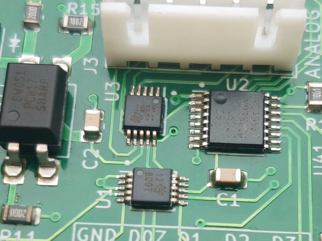
Fine pitch surface-mount soldering 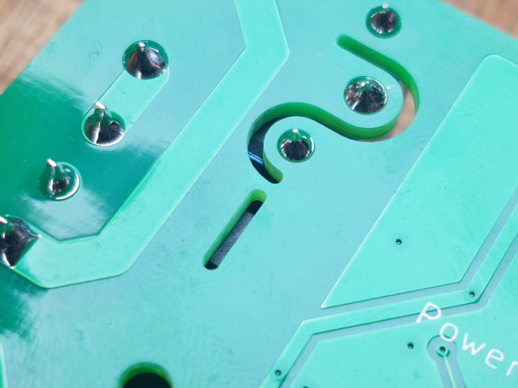
Slot milling and though-hole soldering
The surface mount solder pads look professional and even the tiny 0.2 mm legs of the ADCs were soldered without problems. ICs and diodes are orientated correctly, which can be checked thanks to small marks I added to the silkscreen before. The though-hole components were soldered to the back as they should have, I do not know if they actually used a wave soldering machine or soldered the three boards manually. Either way, all solder joints are shiny and tented indicating a good joint, and the components are flush against the top of the board. Via holes and pads are concentric within a tight tolerance. Silk screen printing is sharp, all designators are readable without problems.
A bit of residual flux was left on some boards, but this was easily wiped away using some alcohol. The green solder mask appears to be thin, but sufficient.
I was curious about their milling capabilities, so I was happy to see that the 1 mm curved isolation slots were precisely cut into the board as I requested. The board edge was also milled as I requested and not v-scored.
In conclusion, I am satisfied with the PCB and assembly quality. Everything has been produced to my precise specifications. The electrical tests confirmed all boards behave as they should, without internal shorts or unexpected side-effects.
Software
Without a capable host controller, this board is pretty much useless. For my first tests, I used my trusty Arduino Uno. I wrote a small library using the Arduino framework and the Wire library, to provide convenient functions for interfacing the board – such that the developer does not have to use the bare I2C interface. The library is hosted on the GitHub project page and also published on the PlatformIO registry.
Since all devices are attached to the I2C bus, the host only has to write the address of a device to the bus and can then follow up with device-specific commands.
The GPIO IC is pretty straight-forward to program for, with essentially a pin map and two pin state registers. The ADCs require a bit more configuration for channel selection, gain and sample rate selection, and they use 16 bit registers. Since the interrupt ready pin of the ADCs is not connected, the host has to check in the status register if a single-shot measurement is done.
For the Raspberry Pi, I used Python 3 and the smbus I2C library. The implementation closely follows the Arduino one and can be found on the GitHub project page.
I am very happy to report that everything works as expected, after designing this PCB using only datasheets and math without actually testing or integrating the components. I can tell you, the first tests were pretty tense!
Thanks
A big thank you to my friend Simon for cross-checking the calculations of the relay drivers.
Special thanks to PCBWay for financially supporting this project and manufacturing it quickly.