Check out the project on GitHub.
In my previous post about NFC security models, I explained why a hardware token that is able to do some computation on its own is required for a secure (enough) authentication. The obvious solution would be to use a YubiKey, however I want to use my own code and control the hardware as well – Especially since I want to target the VivoKey chips in the future.
During my research into NFC hardware, I came across the VivoKey / DangerousThings community and vendor(s), which develop and sell RFID/NFC implants for human use. In-vivo RF implants are nothing new, they have been used in cattle and pets for decades.
Transparency Disclaimer: This project has been in part sponsored by the PCB manufacturing company PCBWay.
Chip Selection
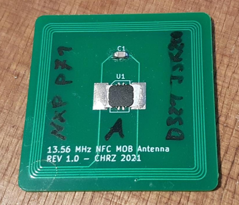
Disregarding the biological side of things, this open-source community also provides a lot of information on the technology used in these types of transponders. For that kind of information I am especially grateful, since e.g. technical details on NXP chips are usually hard to find and/or require non-disclosure agreements to be signed (which I don’t want to do, again, think of open-source). Ultimately, I was able to find a suitable chip, the same one that is used in an upcoming VivoKey product (the VivoKey Apex). This chip is the NXP SmartMX3 P71D321. Public documentation is however, as mentioned before, scarce. Ultimatly, I was able to find the main specs of this chip:
- Manufacturer: NXP Semiconductors
- Series: SmartMX3 Secure and Flexible Microcontroller
- Model: P71D321
- Operating system: JCOP4
- Software interface: GlobalPlatform / JavaCard
- Variant: J3R200 (200KB EEPROM)
- Package: MOB10 ultra-thin
- Hardware interface: Contactless (NFC) only
- Capacitance: 56 pF
In addition, I specified my order to be configured as follows:
- Configuration: “MIFARE Plus EV1 in classic mode 4K applet” removed, leaves 164K EEPROM, 4KB RAM usable
- GlobalPlatform key: 404142434445464748494a4b4c4d4e4f (default test key)
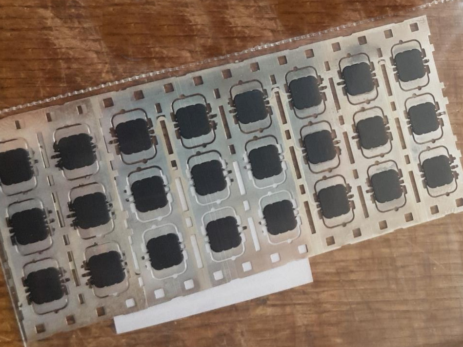
Actually buying the chips proved to be quite a challenge, mainly because NXP does not want to sell their security chips to non-NDA or non-big-industry clients. Kind of understandable, since their products are used e.g. in credit cards. You can buy fully-assembled plastic cards on places like AliBaba or JavaCardOS, but I wanted to buy exactly the chips I specified, without any plastic cards.
Anyway, I had to take a more unofficial route and managed to buy directly from a Chinese factory – turns out a friendly email and sufficient funds go a long way. They sold me off-cuts from the tapes that feed into their pick-and-place machines.
Building PCB Carriers
The next step was to build some circuit boards to actually interface these tiny chips. Specifically, they require a NFC antenna to be attached to their two big solder “pads”. Although I ultimately want to target an implant form factor, I need to somehow test and validate these chips first, since producing flexible implantable PCBs is quite expensive (and also not handled by me personally). I also want to build a testing platform for JavaCard applet development.
Antenna Design
The chip and its attached antenna fundamentally behave like an oscillating LC circuit, the antenna acting as the inductor L and the chip acting as the capacitor C.

The circuit has to resonate at about 13.56 MHz, the center frequency used for NFC. The chip has a nominal capacitance of 56 pF, so with the given target resonance frequency the required antenna inductance works out to be about 2.46 µH. I used this convenient online calculator.

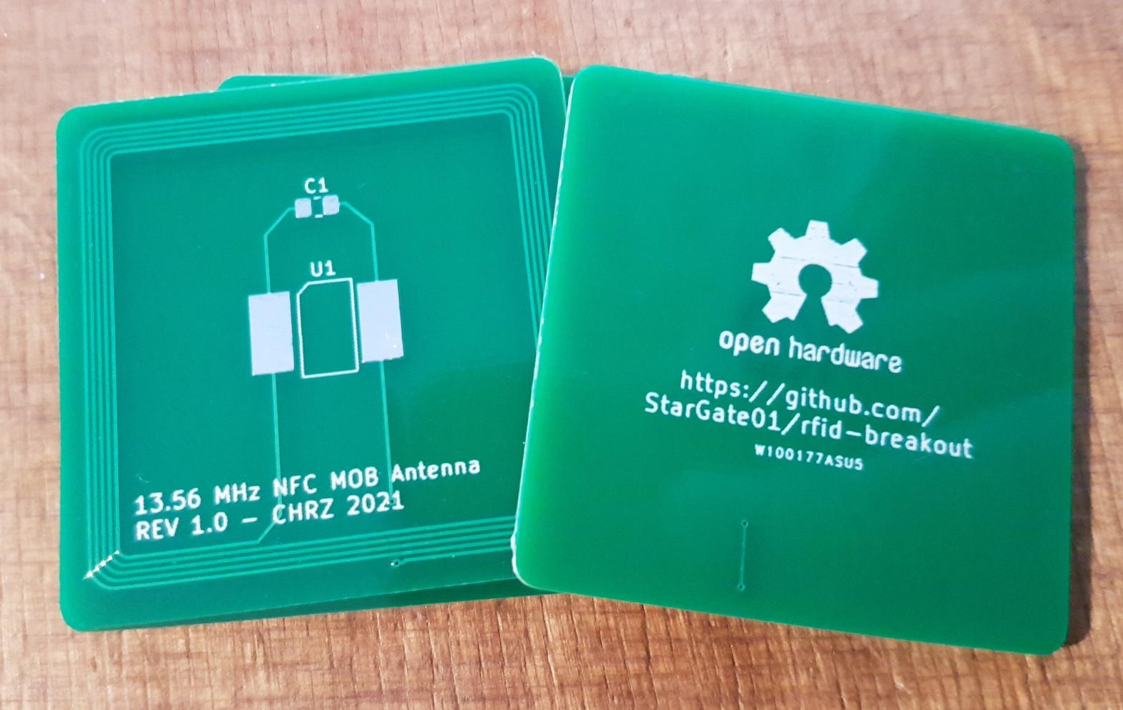
Circuit Board Design
To design the PCB antenna, I used the Coil Inductance Calculation tool written by Satur9 of the DangerousThings community. This tool is based on the application note AN1445 by NXP, specifically pages 46-48.
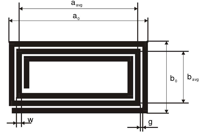
I decided to use a rectangular, spiral, single-sided coil antenna. Referring to the image above, I chose the following parameters.
- Total width (a0): 35 mm
- Total height (b0): 35 mm (square coil)
- Track thickness (t): 0.03556 mm = 1 oz/ft^2
- Track width (w): 0.25 mm
- Track spacing (g): 0.25 mm
- Number of turns (Na): 5
The track thickness, width and spacing were chosen to be well withing the manufacturing capabilities of PCBWay, while still keeping the PCB small. The number of turns recommended by the application note is 1 – 6, so i figured 5 would be fine. The size was found by trial and error, until I hit the required inductance.
As per the calculator and the application note, this design gives the coil a theoretical inductance of 2.196 µH . But that is quite a bit off from the target inductance of 2.46 µH, as you might notice. However, this undershoot is by design. In the real world, no PCB is perfect. There may be manufacturing tolerances that slightly skew the traces, and parasitic capacitance and inductance may be a problem as well. And I have not even accounted for the rounded corners in my design yet.
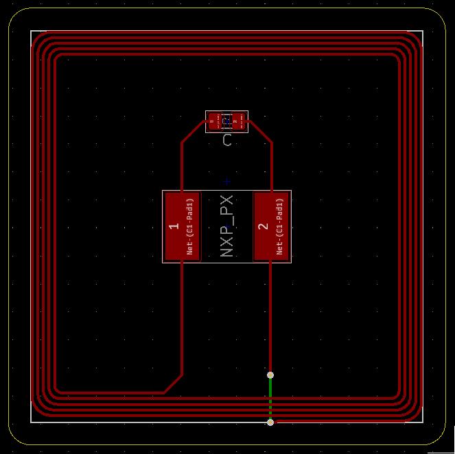
To fix this, I added a footprint for a parallel capacitor (C1) to my PCB design. This capacitor will increase the capacitance of the chip circuit, allowing it to resonate at the target frequency using the lower-inductance antenna. This approach was chosen because it is easy to add additional capacitance, in comparison to removing capacitance or even modifying the inductance.
Using the designed coil with the undershot inductance of 2.196 µH, the required capacitance to hit the 13.56 MHz resonant frequency works out to be about 62.73 pF. This is 6.73 pF more than the capacitance of the chip, so we should be adding that for C1 theoretically. If some real-world effects influence the circuit, we can always compensate and choose a different capacitor.
PCB Manufacturing
The company PCBWay sponsored and manufactured the PCBs for this project. I am very grateful for their support, and the PCBs I received once again met my expectations and performed well. As it will turn out later, my calculations were pretty close – which speaks for their precision in manufacturing.
I had to explicitly specify for the manufacturer to etch away all the copper on the backside, except the one little trace, and to not apply any soldermask. This seems to be a rather unusual case, but it is very much required for my design – because the antenna won’t work with a large copper backplane next to it.
Antenna Evaluation
To choose the correct value for C1, I first had to measure the current resonant frequency of the circuit without any capacitor added. To measure this frequency, I used a vector network analyzer, specifically the NanoVNA. This smart device essentially performs a frequency sweep and records the frequency response of the device under test. It then is able to construct e.g. a Smith chart or SWR (standing wave ratio) plot.
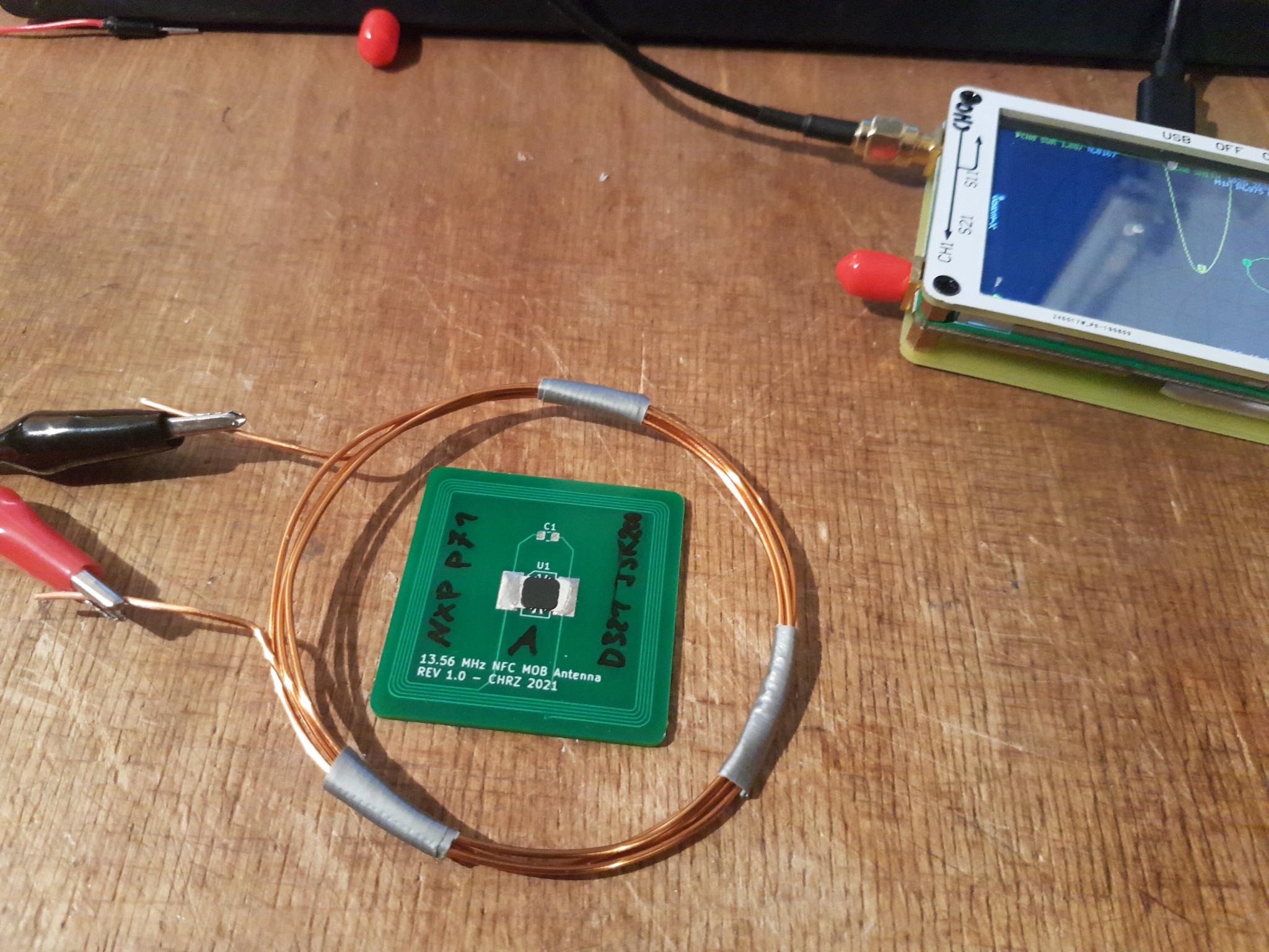
I calibrated and set up the NanoVNA to perform sweeps from 10 MHz to 20 MHz, and recorded the reflection on channel zero. At the resonant frequency of the PCB, the energy reflected should be the lowest, as the PCB sinks RF energy when it is properly frequency-coupled.
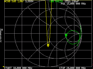
Using the measured frequency and the assumed capacitance of 56 pF, the corresponding inductance of the circuit computes to be about 2.010 µH – not even that far off from the theoretical value. Plugging this inductance back in, and computing the required capacitance to hit the correct frequency of 13.56 MHz, the correct total capacitance turns out to be about 68.525 pF. This means that C1 should be about 12.5 pF. The closest SMT component I have is a 10 pF capacitor, which should be good enough since these SMT capacitor values are not even that precise usually.
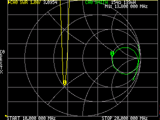
After adding the capacitor, the resonant frequency is within a range of 300 KHz from the target frequency of 13.56 MHz, which is good enough to establish a solid connection with commercial NFC readers.
Software
I used my SCL011 PC/SC-compliant NFC reader to interface with the PCBs. The range in which the reader was able to communicate with the chips turned out to be pretty good, about 2 – 3 centimeters. My phone is also able to interface with the PCBs without issues.
For programming, I used the GlobalPlatformPro tools, which enabled me to load my compiled JavaCard applets onto the chip. I successfully tested the following applets, simultaneously:
- vk-ykhmac (Tested with KeepassXC, and Keepass2Android & ykDroid): https://github.com/StarGate01/vk-ykhmac
- Flex-OTP (Tested with 21 separate entries; Modified by me to impersonate an original YubiKey to work with the YubiKey Authenticator apps): https://github.com/StarGate01/Flex-OTP
- Flex-SmartPGP (Tested with GnuPG & Thunderbird, Kleopatra & Outlook, and OpenKeychain & K9-Mail): https://github.com/ANSSI-FR/SmartPGP
- openjavacard-ndef (Tested with 2048 bytes r/w storage): https://github.com/OpenJavaCard/openjavacard-ndef
Conclusion
This project proved to be a successful evaluation of the NXP P71 chip. I also was able to verify that several applets are able to run on the chip, and that my various devices can interface with them.
A special thanks goes out to Satur9, rileyg, NiamhAstra/Miana and the rest of the DangerousThings community for their help with this project.
Check out the hardware design files on GitHub.
Thank you for your hard work and through documentation, I have had as much enjoyment reading it.